
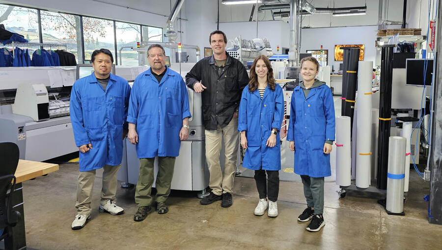
About Us
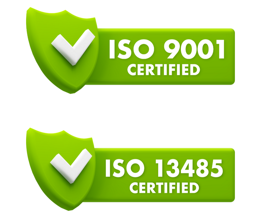
Bay Area PCB Assembly offers a comprehensive printed circuit board assembly service that covers every aspect of the process, from initial part procurement to final shipping. Utilizing a blend of cutting-edge technology and skilled craftsmanship, we ensure precision and quality at every step. The service includes meticulous planning based on an approved Bill of Materials (BOM), precise solder paste application, automated and manual component placement, and a variety of soldering methods tailored to each project's unique requirements. Advanced inspection techniques, such as [3D Automated Optical Inspection AOI and X-Ray technology, are employed to guarantee the highest quality standards. The end result is a meticulously assembled PCB, cleaned and packaged with industry-standard materials, ready for immediate integration into your projects. We are ISO 9001 and 13485 certified.
Services
Our expertise extends to a range of specialized services:•Custom Printed Circuit Board Design: Tailored to your specific needs, ensuring high performance and reliability.•Precision PCB Assembly: Meticulous assembly processes to bring your designs to life with exceptional accuracy.•Advanced X-Ray Inspection: Utilizing cutting-edge technology to ensure the highest quality and integrity of your PCBs.PCB Repair: Our technicians can do PCB repair on a case by case basis. Contact us for a consultation.

Testimonials

Working with this Bay Area PCB Assembly has been an exceptionally smooth experience. They have clearly invested heavily in their PCB equipment and have a talented team dedicated to designing and manufacturing high-quality products. Throughout my project, their communication was commendable. They consistently kept me informed with detailed updates at each stage, ensuring that I was always in the loop. It never felt like I was taking a risk and was a great experience overall. I look forward to working with them in the future.-Manny Bains

Photon Ink has been working with Bay Area PCB Assembly for several years and their service is unmatched. Myles and his team are easy to work with, flexible and quick to respond. They strive to please their customers and never cease to meet our needs and expectations.
-Kristie Brown

We developed a breadbot to make fresh bread in stores. We had issues with our old control system, so went to Sam and the team to design and build a custom PCB system and software package. They designed and built a perfect solution from pcb to cloud. We are very happy with the final product and have had almost zero issues in the field with the boards. We work with hundreds of suppliers and Sam and team are by far the best. They understand their domain and are great to work with. I would highly recommend.
-Eric Wilkinson


FAQs
What's your process?
Our PCB assembly process is outlined here.Are you ISO certified?"
Yes, we are ISO 9001 and 13485 certified.What are some of the equipment you use?
A list of the equipment we use for our PCB Assembly can be found here.Do you offer X-Ray inspection?
Yes we do. We employ 2D and 3D imaging technologies to accurately identify assembly defects and perform in-depth analysis on PCBs, ensuring swift and consistent inspections powered by YXLON Cheetah EVO technology.Do you perform work to IPC standards?
Yes, our work is performed to IPC standards.What's your contact information?
Our phone number is (916) 692-9706 or you can drop us a message hereWhat are your traceability capabilities?
A description of our advanced traceability capabilities can be found hereWhere are you located?
Our address is
5175 Hillsdale Cir Suite 150, El Dorado Hills, CA 95762Can we take a tour of your facility?
Yes, call us at (916) 692-9706 to arrange a tour.

Our Process
1. PROCUREMENT AND PLANNING
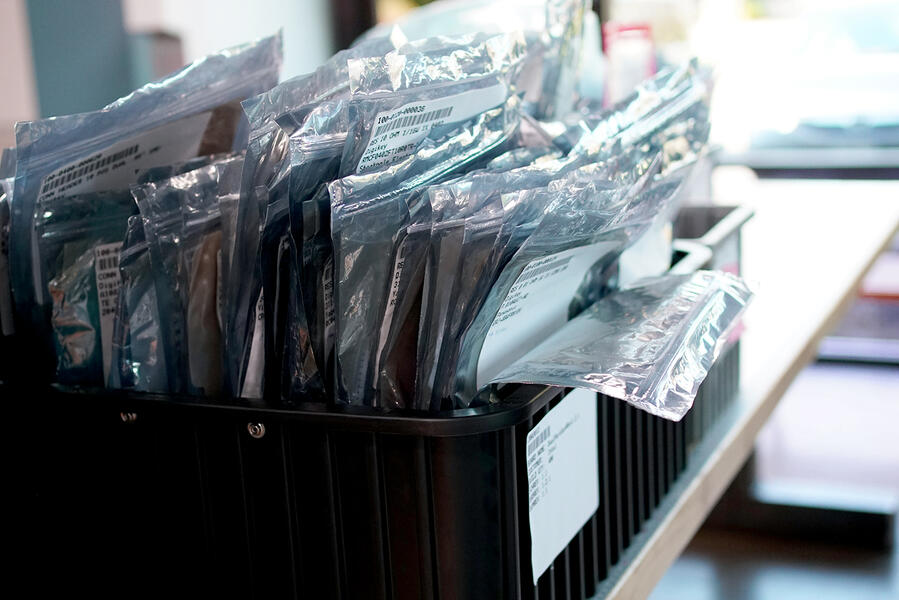
Starting a PCB project kicks off with acquiring the necessary parts. After the project's specifications are set, we source the components and create a Bill of Materials (BOM), detailing each component, its manufacturer, and delivery information. Once you approve the BOM, we order the parts. Your project officially starts when these parts arrive. Upon arrival, we categorize the parts by project, scan them into our system, and track them during the PCB assembly. This meticulous process guarantees precise component placement and allows us to pinpoint and resolve any issues efficiently.
2. SOLDER PASTE
Before attaching components to a PCB, solder paste must be precisely applied to specific areas, primarily the component pads. This paste is a mixture of metal alloy powder and flux, a putty-like substance, and applying the right amount is critical to avoid misalignments or poor connections. There are two methods for this: using a solder screen or a jet printer. The solder screen, created during the board design process, has holes aligned with the board's solder-required areas. Paste is spread over the screen and then scraped through the holes to the board. In contrast, a jet printer, which is like a conventional printer, receives coordinates for where to apply paste and precisely deposits it in tiny dots on the component pads. While jet printers are more accurate and reduce solder waste, they are not as quick as the screen printing technique.
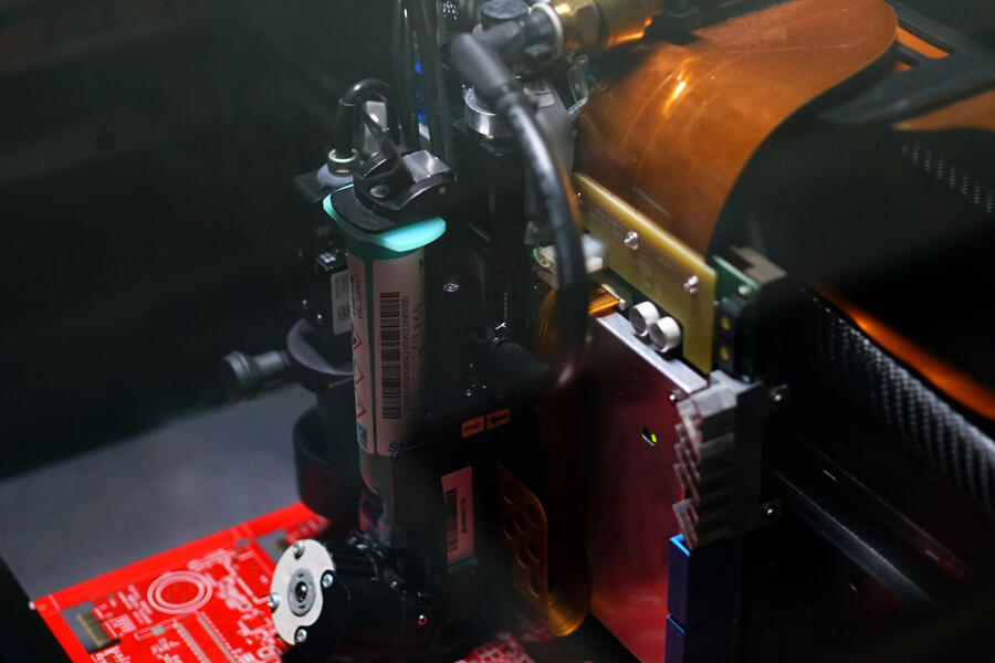
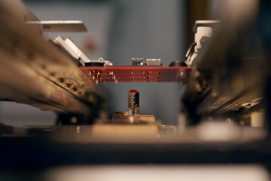
3. COMPONENT PLACEMENT
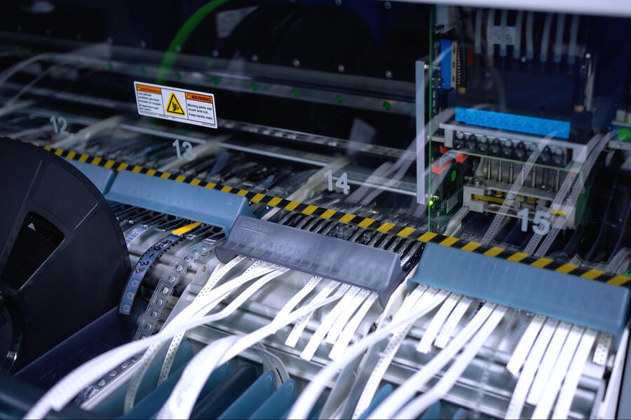
Following the solder paste application, boards now termed 'wet boards' are ready for component placement. While some larger or through-hole components are manually placed, most components are positioned onto the board using pick and place machines. These machines function as their name implies: they pick up each component and place it accurately on the board. Components are loaded into the machine in reels, and using specialized software, the precise location and orientation of each part are programmed. During operation, one or multiple heads of the machine pick up the components, align them as per the design specifications, and place them onto the wet solder. This holds the components temporarily in place until they are permanently affixed through the soldering process.
4. SOLDERING
After a board is fully assembled with components, the next step is to melt the solder to permanently attach these parts to the board. This process varies based on the component's size, placement, and type, and can be done through hand soldering, reflow ovens, or selective soldering methods. In reflow ovens, boards are moved on conveyor belts through various heating and cooling zones. Technicians tailor the conveyor's speed and the temperature in each zone to create specific time-temperature profiles, ensuring the solder melts as needed for each specific project. Selective soldering, on the other hand, involves a nozzle guided by a set of coordinates to apply a targeted molten solder fountain to unsoldered components. This method is particularly useful for parts that need soldering after initial reflow oven processing, requiring precision to avoid damaging adjacent, already soldered parts. If selective soldering isn't suitable, our skilled technicians undertake hand soldering, using state-of-the-art Metcal soldering equipment, to ensure the highest quality in PCB assembly.
5. INSPECTION
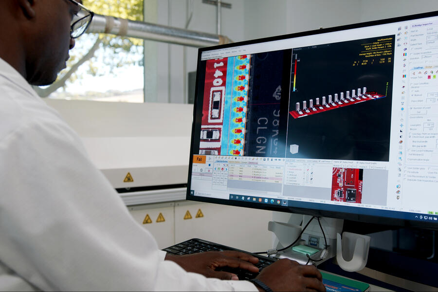
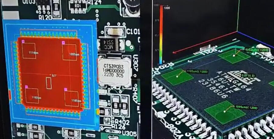
Inspections in PCB production are integral and occur at multiple stages, including key Automated Optical Inspection (AOI) checks on wet boards for solder paste. However, the bulk of inspections are conducted post-completion, as manual checking of surface mount boards with extensive components is impractical. Instead, 3D AOI and X-Ray technologies are utilized for thorough analysis. AOI uses intense light flashes to reveal imperfections and read part numbers, quickly assessing each component's presence, location, and orientation, and detecting issues like bent or lifted leads with its volumetric height measurement. X-Ray inspection, essential for uncovering internal defects and examining parts hidden by others, employs non-destructive techniques. While 2D X-Ray excels in individual board or component examination, particularly for void analysis, 3D X-Ray takes thousands of images to reconstruct detailed views of whole or parts of boards and components, ensuring even the smallest elements are meticulously inspected.
6. CLEANING, PACKING, AND SHIPPING
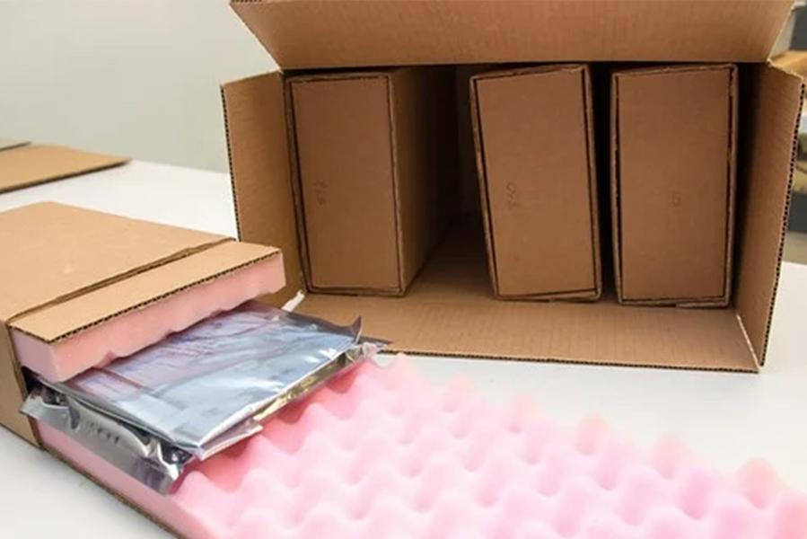
Once all required components are sourced, soldered onto the boards, and the boards have successfully passed all necessary inspections, they are nearly set for dispatch. The final step involves a gentle cleaning process to eliminate any residual solder paste, glue, or other substances acquired during assembly. After this, the boards are meticulously packaged using industry-standard, antistatic materials, ensuring their safe and secure delivery to the customer.

Our Equipment
Bay Area PCB Assembly utilizes an array of top-tier machinery to facilitate both the assembly and quality inspection of each project.
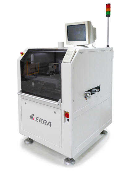
Asys Group Ekra X4
The EKRA X4, by ASYS Group, is a high-precision automatic screen and stencil printer tailored for diverse production demands within the electronics industry, with a notable ease of use and flexibility. It's engineered for precise application of solder paste and/or glue onto substrates like PCBs, ceramics, or glass, within a printing area of 460 x 460 mm. The EKRA X4 boasts quick reconfiguration, facilitated by a user-friendly interface and simple programming, alongside a patented optical positioning system for accurate material application. Its robust construction ensures stability, while specifications like a power rating of 230V 50/60Hz 2.0 kW 16 Amp, two pneumatically driven print heads, and a quick product changeover in less than 5 minutes underscore its efficiency and user-centric design. Additional features like variable stencil pickup, optical solder paste detection, and Grid-Lock PCB support enhance its functionality, making it a reliable choice for high-efficiency, precise printing in the electronics industry.
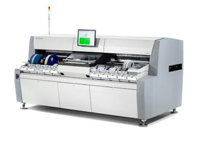
Mycronic MY600 Jet Printer
The Mycronic MY600 Jet Printer is a cutting-edge device designed for stencil-free solder paste application on PCBs, optimizing both speed and precision in the process. With the ability to dispense over one million dots of solder paste per hour, it achieves a 50% increase in throughput compared to earlier models. The MY600 operates with micrometer accuracy, even at high speeds, handling complex boards efficiently by optimizing paste volume for each solder joint using non-contact technology. Its sophisticated system calculates the trajectory of each dot in real-time, akin to a plane determining when to drop a bomb, thus allowing continuous printing at a pace of 600 dots every second without pause, significantly accelerating the PCB assembly process while ensuring high-quality solder joints on challenging circuit boards and components.
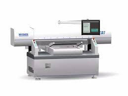
Mycronic MY300ex
The Mycronic MY300EX is a cutting-edge device designed for stencil-free solder paste application on PCBs, optimizing both speed and precision in the process. With the ability to dispense over one million dots of solder paste per hour, it achieves a 50% increase in throughput compared to earlier models. The MY600 operates with micrometer accuracy, even at high speeds, handling complex boards efficiently by optimizing paste volume for each solder joint using non-contact technology. Its sophisticated system calculates the trajectory of each dot in real-time, thus allowing continuous printing at a pace of 600 dots every second without pause, significantly accelerating the PCB assembly process while ensuring high-quality solder joints on challenging circuit boards and components.
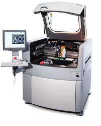
Mycronic MY9
The Mycronic MY9 is a distinguished pick-and-place machine tailored for efficient surface mount technology (SMT) assembly. Its core strength lies in precision placement, reducing material waste while maximizing production yields. Designed for speed, the MY9 accelerates component handling and placement rates without sacrificing accuracy, crucial for adhering to stringent production schedules. It showcases versatility in handling a broad spectrum of SMT components, making it apt for both standard and complex assembly tasks. The user-friendly interface simplifies operations, minimizing downtime and ensuring a swift learning curve in bustling production settings. An integrated automated vision system autonomously aligns and corrects component positions before placement, significantly lowering error margins and upholding consistent quality output. The MY9 is engineered for seamless integration with other assembly line machinery, promoting an efficient, synchronized production flow. Additionally, its expandable configurations allow it to adapt to evolving production demands, displaying a future-ready approach. With an eye on sustainability, the MY9 operates with energy efficiency and waste reduction at its core, aligning with modern sustainable manufacturing mandates. The functional prowess of the Mycronic MY9 makes it a robust, pragmatic choice for those keen on optimizing their SMT assembly processes.
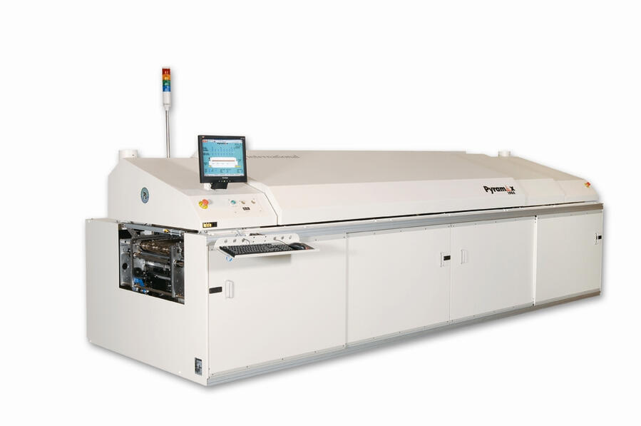
BTU International Pyramax 98
TheBTU International Pyramax 98 is a sophisticated forced convection lead-free reflow oven, designed to excel in high-demand manufacturing environments. It features 7 vertical heating zones with top and bottom heaters, ensuring precise temperature control throughout the solder reflow process, and a maximum temperature capacity of 350°C for high-temperature applications. Enhanced by the integration of the SuperM.O.L.E.® Gold 2 Thermal Profiler, the oven allows for the creation of precise, custom oven profiles, ensuring optimal performance tailored to specific needs. The unit also includes a dedicated cooling zone with two-speed control blowers, a combination of Pin-Chain and Centre Board Support Conveyor system, and an adjustable width conveyor setup, accommodating various board sizes and ensuring smooth material transit. Operating on a 208V or 440V, 3 Phase power supply, the Pyramax 98 stands as a reliable and versatile choice for a myriad of solder reflow requirements.
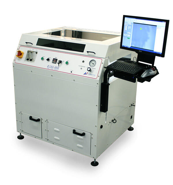
ACE KISS 101
The ACE KISS 101 is a selective soldering system adept at soldering through-hole components on Surface Mount Technology (SMT) boards, especially beneficial when the components are near adjacent parts. It curtails manual soldering challenges and labor costs through an automated molten solder delivery system, further enriched by a range of programmable features allowing precise control over process parameters such as flux deposition, immersion depths, and solder temperature. With its high throughput, it's capable of outperforming multiple operators, while also offering an array of standard and custom nozzles for varied soldering needs. The system, known for its ruggedness, supports lead-free solder, making it suitable for low to medium volume assembly operations. The KISS 101B variant comes with ACE KISS Teach 2.0 software for enhanced process control and monitoring, presented as a low-cost, user-friendly, free-standing, and CE-compatible model, signifying its compliance with crucial safety and performance standards, ideal for quick-turn rework or light assembly facilities.
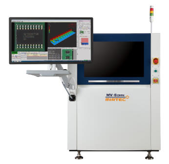
Mirtec MV-6 OMNI
The Mirtec MV-6 OMNI is engineered to boost productivity in the inspection of Printed Circuit Board Assemblies (PCBA) through its high-speed, high-performance 3D Automatic Optical Inspection (AOI) capabilities. Key features include a 15 Mega Pixel CoaXPress Camera Technology for detailed imaging, an advanced Eight Phase Color Lighting System for enhanced defect detection, and a 10 Micron/Pixel Precision Telecentric Compound Lens Design for accurate imaging. Additionally, it boasts an Integrated Ten Mega Pixel SIDE-VIEWER® Camera System for comprehensive inspection from different angles, Non-Blind Spot Digital 8 Projection Moiré 3D Inspection Technology for precise component and micro crack detection, a Precision Closed Loop AC Servo Drive Motor System for exact operation, and user-friendly programming and operation functionality, making it a reliable and robust tool for thorough PCBA inspection.
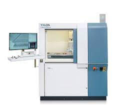
YXLON Cheetah Evo
The YXLON Cheetah EVO is a robust inspection system optimized for detailed examination, particularly in electronics. Its large flat-panel detectors enhance the field of view by up to 50%, expediting automated processes. With high-resolution inspection capabilities, it employs dynamic image enhancing filters like eHDR for refined imagery. The system harbors advanced technologies like FeinFocus X-ray tube and High Power Target technology for superior 2D and 3D imaging. It's ready for Industry 4.0, featuring integrated workflows and automated software solutions like the Comet Yxlon FF CT and YXLON ProLoop for real-time reporting and faster visualization. The intuitive workflow facilitates easy programming of automated procedures, and its flexibility is showcased in three models catering to varied inspection needs, demonstrating its adaptability in modern inspection scenarios.

Precision with Advanced Traceability
At Bay Area PCB Assembly, we're revolutionizing the electronics manufacturing industry with our state-of-the-art traceability capabilities. Our commitment to precision and reliability is evident in every Printed Circuit Boards (PCBs) we assemble. Let's explore how our sophisticated traceability methods are setting new standards in PCB assembly.Enhanced Batching and Component VerificationOur journey towards unparalleled precision begins with an innovative batching process. As components arrive to be mounted on circuit boards, they're assigned a unique batch number, and a photograph of the component package is taken, displaying part numbers. This system links each batch to its specific purchase order and receipt from our trusted authorized distributors, ensuring complete traceability for every component we use.Unique PCB Serialization for Complete TraceabilityAt the heart of our traceability system lies the unique serialization of each PCB. Every board we produce at Bay Area PCB Assembly is given a distinct serial number, creating a traceable identity that is essential for maintaining high standards of accountability and quality.Automated Component Placement and DocumentationUtilizing the latest in automated technology, our equipment meticulously documents and stores the batch number for every component placed on each uniquely serialized PCB. This extends to measuring resistor and capacitor values before placement, allowing for actual values to be documented and reviewed in the future. This attention to detail ensures that every component on each PCB is precisely traceable.The Traveler System: A Testament to Our Commitment to QualityOur traveler system is a testament to our dedication to quality. It begins with a cover sheet listing the primary specifications for PCB assembly, including IPC Class adherence and RoHS or ITAR compliance. Every process in the PCB assembly is documented, with our skilled technicians signing and dating each step upon completion. These documents are scanned and stored in our database, offering a detailed and retrievable record of the entire assembly process.Advanced AOI Inspection for Flawless Quality AssuranceOur Automated Optical Inspection (AOI) system is a cornerstone of our quality assurance process. It not only captures images of each inspected PCB linked to its unique serial number but also uses optical character recognition to validate branding marks on ICs against component datasheets. This meticulous inspection ensures that only the correct components are used, upholding our commitment to flawless quality.Comprehensive Traceability: The Bay Area PCB Assembly AdvantageTo summarize the robustness of our system: Every component, ordered according to the Bill of Materials, is traced right from its batch number to its placement on the PCB. Our advanced equipment precisely places each component, recording all necessary details. Post-assembly, our AOI system thoroughly inspects and documents each component on the finished boards.This comprehensive traceability enables us at Bay Area PCB Assembly to provide detailed information about any component on a PCB, even if it was assembled years ago. Whether it's retrieving images of the component batch, purchase history, or its exact placement on the PCB, our system ensures that this information is just a query away.In conclusion, the advanced traceability capabilities at Bay Area PCB Assembly epitomize our dedication to delivering precision, reliability, and transparency in electronics manufacturing. By meticulously tracking every component and process, we provide our clients with the highest quality standards and peace of mind in their electronics manufacturing endeavors.
Blog
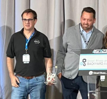
Ansync Labs Awarded Ecosystem Builder Award
Ansync Labs, the parent company of Bay Area PCB Assembly, has been recognized with the Ecosystem Builder Award at the GFX2023 Backyard Awards. This award is a tribute to organizations that dedicate resources, time, and expertise towards nurturing a flourishing entrepreneurial ecosystem for the benefit of founders and the wider regional community.Located in Northern California, Ansync Labs is a design for manufacture firm that adopts a multidisciplinary approach towards solution development, iteration, and product realization. Our team of electrical, software, and mechanical engineers, backed by an in-house machine shop and electronics assembly line, strives to contribute meaningfully to practical solution delivery. Our endeavors span across motors and automation, medical, and IoT devices, areas where we hope to make a positive impact.The GFX2023 Backyard Awards, facilitated by Growth Factory and supported by Stoel Rives, is a heartfelt initiative that acknowledges the significant work being done locally, particularly in the Greater Sacramento area. Amid a world often focused on global events, this event brings attention to the meaningful contributions occurring right within our community.Being honored with the Ecosystem Builder Award is a gentle reminder of the importance of our mission to support the entrepreneurial ecosystem of the region. This recognition is not a destination but a milestone that encourages us to continue our efforts with renewed vigor. It also serves as a modest example for other organizations, showcasing the potential for positive contributions to our local entrepreneurial environment. While we are thankful for this recognition, it further motivates us to continue our work, fostering a nurturing environment for entrepreneurship within our community, and contributing towards a brighter and more innovative future for all.
Blog
Getting It Built: Moving from Prototype to Production
In the bustling world of startups, taking a product from prototype to production is often seen as a daunting task. It's a convoluted process that involves a slew of variables, from securing funding to managing supply chains. Sam Miller, the founder of Ansync Labs, presented to Startup Grind Sacramento on [Getting It Built: Moving from Prototype to Production. Here's what he covered:The Challenge of Funding and MarketingAccording to Miller, startups often find themselves in a conundrum when it comes to securing sufficient funding. They either miscalculate the required budget or run out of resources before reaching the end goal. The solution? A meticulously designed financial plan that incorporates room for setbacks and pivots.As Miller noted, marketing isn't a secondary concern; it's integral to the product development process. You need to be clear about who your target customers are and how you're going to reach them, ensuring your marketing and sales strategies are airtight.Vendor Relationships: The Unseen BackboneOne of the vital aspects Miller stressed was the importance of establishing strong vendor relationships. Whether it's custom screws or advanced electronic components, finding the right vendor can be a game-changer. He advocated for a strategy that cultivates long-term, mutually beneficial relationships with vendors. This involves diligent research, vetting, and ongoing communication to ensure quality and reliability.The Balancing Act: Overseas vs. Domestic ProductionShould you manufacture your product domestically or offshore it overseas? According to Miller, the answer lies in a balance. High labor portions of your product can be produced more cost-effectively overseas, while more complex or sensitive components might be best manufactured domestically. The key is to carefully consider factors like shipping costs, tariffs, and quality control, thereby striking a balance that aligns with your production goals and values.The Importance of Tolerances and SpecificationsIn Miller's view, a detailed and accurate specification sheet is worth its weight in gold. By providing vendors with precise tolerances and requirements, you minimize misunderstandings, reduce costly errors, and ensure the final product meets quality standards. It's about not leaving room for assumptions, thus preventing future headaches.The Concept of a 'Supply Funnel'Miller introduced the notion of a 'Supply Funnel,' explaining that products are built in stages, moving from individual components to sub-assemblies and finally, to the finished product. Effective management of this funnel can lead to streamlined operations and a faster time-to-market. The strategy here is to identify which components can be outsourced, how they will be assembled, and where the final product will be made, optimizing each step of the supply funnel for efficiency and cost-effectiveness.In conclusion, transitioning from a prototype to a production-level product is no small feat. But with clear planning, strong vendor partnerships, and a well-calibrated balance between domestic and overseas production, startups can navigate this complex journey more efficiently. As Sam Miller effectively demonstrated, it's not just about getting it built; it's about getting it built right.
Blog
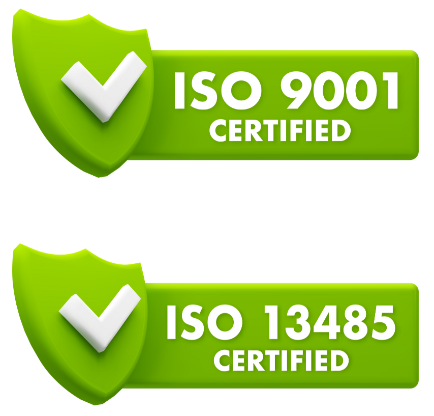
Press ReleaseBay Area PCB Assembly Achieves ISO 9001 and ISO 13485 CertificationsFOR IMMEDIATE RELEASEFolsom, CA – August 8, 2024 – Bay Area PCB Assembly, a leading provider of printed circuit board (PCB) assembly services, is proud to announce that it has been awarded ISO 9001:2015 and ISO 13485:2016 certifications. These prestigious certifications underscore our commitment to quality management and dedication to meeting the rigorous standards of the medical device industry.The ISO 9001:2015 certification is an internationally recognized standard that ensures the company's quality management system (QMS) consistently provides products and services that meet customer and regulatory requirements. This certification reflects Bay Area PCB Assembly's continuous improvement and customer satisfaction efforts.The ISO 13485:2016 certification specifically addresses the stringent requirements for a comprehensive QMS for the design and manufacture of medical devices. Achieving this certification demonstrates Bay Area PCB Assembly's ability to provide high-quality PCB assemblies that meet the exacting standards of the medical device industry."We are extremely proud to have achieved both ISO 9001 and ISO 13485 certifications," said Sam Miller , CEO of Bay Area PCB Assembly. "These certifications are a testament to our team's hard work, dedication, and commitment to excellence. They also reinforce our ability to deliver top-tier PCB assembly services to our clients, particularly in the medical device sector."Bay Area PCB Assembly has consistently focused on quality, innovation, and customer satisfaction. With these certifications, the company is well-positioned to expand its market presence and continue delivering reliable and high-quality PCB assemblies to its growing customer base.For more information about Bay Area PCB Assembly and its services, please visit www.bapcbassembly.comMedia ContactRich Foreman
Marketing Consultant, Bay Area PCB Assembly
Email:[email protected]About Bay Area PCB AssemblyBay Area PCB Assembly is a premier provider of PCB assembly services, offering a wide range of solutions to various industries, including medical, aerospace, and consumer electronics. With a strong emphasis on quality, innovation, and customer satisfaction, the company is dedicated to delivering exceptional products and services that meet the highest industry standards.
About Us
Bay Area PCB Assembly offers a comprehensive printed circuit board assembly service that covers every aspect of the process, from initial part procurement to final shipping. Utilizing a blend of cutting-edge technology and skilled craftsmanship, we ensure precision and quality at every step. The service includes meticulous planning based on an approved Bill of Materials (BOM), precise solder paste application, automated and manual component placement, and a variety of soldering methods tailored to each project's unique requirements. Advanced inspection techniques, such as [3D Automated Optical Inspection AOI and X-Ray technology, are employed to guarantee the highest quality standards. The end result is a meticulously assembled PCB, cleaned and packaged with industry-standard materials, ready for immediate integration into your projects.
5175 Hillsdale Cir. Suite 150
El Dorado Hills, California 95762
Bay Area PCB Assembly is a division of Ansync Labs headquartered in El Dorado Hills, California. We serve the Bay Area including San Francisco, Alameda, Albany, Berkeley, Dublin, Emeryville, Fremont, Hayward, Livermore, Newark, Oakland, Piedmont, Pleasanton, San Leandro, Union City, Antioch, Brentwood, Clayton, Concord, Danville, El Cerrito, Hercules, Lafayette, Martinez, Moraga, Oakley, Orinda, Pinole, Pittsburg, Pleasant Hill, Richmond, San Pablo, San Ramon, Walnut Creek, Belvedere, Corte Madera, Fairfax, Larkspur, Mill Valley, Novato, Ross, San Anselmo, San Rafael, Sausalito, Tiburon, American Canyon, Calistoga, Napa, St. Helena, Yountville, Atherton, Belmont, Brisbane, Burlingame, Colma, Daly City, East Palo Alto, Foster City, Half Moon Bay, Hillsborough, Menlo Park, Millbrae, Pacifica, Portola Valley, Redwood City, San Bruno, San Carlos, San Mateo, South San Francisco, Woodside, Campbell, Cupertino, Gilroy, Los Altos, Los Altos Hills, Los Gatos, Milpitas, Monte Sereno, Morgan Hill, Mountain View, Palo Alto, San Jose, Santa Clara, Saratoga, Sunnyvale, Benicia, Dixon, Fairfield, Rio Vista, Suisun City, Vacaville, Vallejo, Cloverdale, Cotati, Healdsburg, Petaluma, Rohnert Park, Santa Rosa, Sebastopol, Sonoma, Windsor